Wireless Charging For Your Mobile Phone
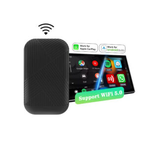
What is Wireless Carplay adapter?
Regarding the Wireless CarPlay adapter, let’s first understand CarPlay. What is Carplay? In the center console of a car, there
With the continuous development of human society, the continuous advancement of science and technology, the popularization of smart phones has brought people an unprecedented technological experience. Smart phones have fast power consumption, short battery life, interface damage caused by frequent charging, and power banks are inconvenient to carry, etc. The problem also ushers in an opportunity for the development of mobile phone wireless chargers.
Since the iPhone 8 mobile phone also has the function of wireless charging, the wireless charger market for iPhone mobile phones has opened up rapidly, and various new wireless charger styles and functions have been gradually invented. More and more wireless chargers have entered our field of vision. Among them, what is the production process of the wireless charger, and what is its internal structure? Today, I will take you to understand the production process of the wireless charger in the form of pictures, texts, and videos.
The wireless charger is mainly composed of three parts: the main board, the coil and the shell. The main board directly determines the function and performance of the wireless charger and is the core module of the wireless charger. The motherboard is mainly composed of a main control chip, a driver chip, a power device (MOS), resistors and capacitors, and a PCB board.
Among them, the main board directly determines the function and performance of the wireless charger, and is the core module of the wireless charger. The motherboard is mainly composed of a main control chip, a driver chip, a power device (MOS), a resistor and a capacitor, and a PCB board. The coil is generally a standard module, and the relevant wireless charging standards strictly stipulate its structural size parameters.
Energy can be efficiently transmitted between two objects with the same resonant frequency, while the interaction between objects with different frequencies is weak. Wireless charging technology takes advantage of this principle. Similarly, wireless charging technology also applies the principle of electromagnetic wave induction and related AC induction technology. It uses corresponding coils at the sending and receiving ends to send and receive induced AC signals for charging.
Current flowing through the coil creates a magnetic field. Other non-energized coils will generate current when they are brought close to the magnetic field. Wireless charging applies this physical phenomenon by arranging coils that can resonate with magnetic field vibrations to extend the power supply distance.
First, design the appearance of the product in the design software, build the structural detail model in the modeling software, and then render the material of the product.
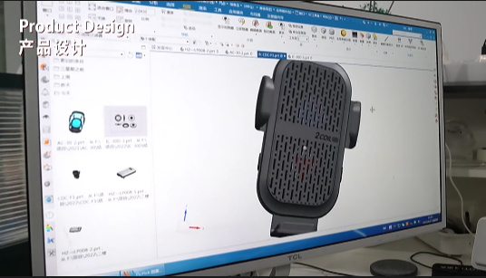
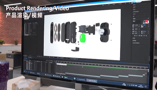
After the shell is designed, you can open the film and inject the shell to produce the shell, and prepare the spare parts of the shell (screws, buttons, charging lines)
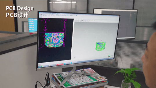
After designing the PCB board, design the solder paste printing stencil according to the size and circuit required by the circuit components, and start printing the solder paste.
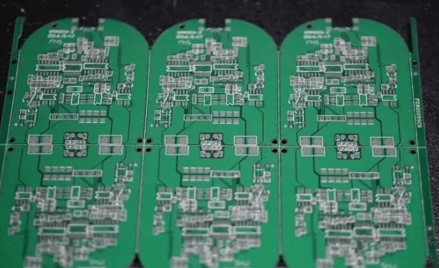
The picture above is an empty board without any electronic components. First, it will be placed on a fully automatic printing machine and painted with a layer of solder paste. Solder paste is made by mixing solder powder, flux and other surfactants and thixotropic agents. It can be seen from the picture that there are more than 30 components in this wireless charger circuit board.
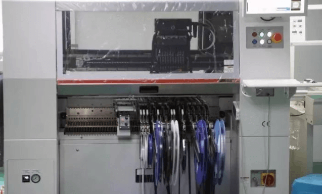
Each SMT high-speed placement machine will be controlled by a small computer. The engineer will design the capacitor resistor chip material for each wireless charging circuit board, and the computer will program the preset operating procedures, which greatly improves the placement of the circuit board. slice accuracy.
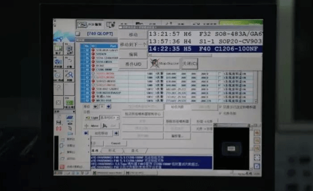
The installation of electronic components has a fixed position and order, as shown in the lower right corner of the figure, the chip is being installed.
The installed circuit board enters the reflow soldering machine for reflow soldering. The so-called reflow soldering is to blow heated air or nitrogen to the circuit board with installed components to connect the circuit.
The installed circuit board enters the reflow soldering machine for reflow soldering. The so-called reflow soldering is to blow heated air or nitrogen to the circuit board with installed components to connect the circuit.
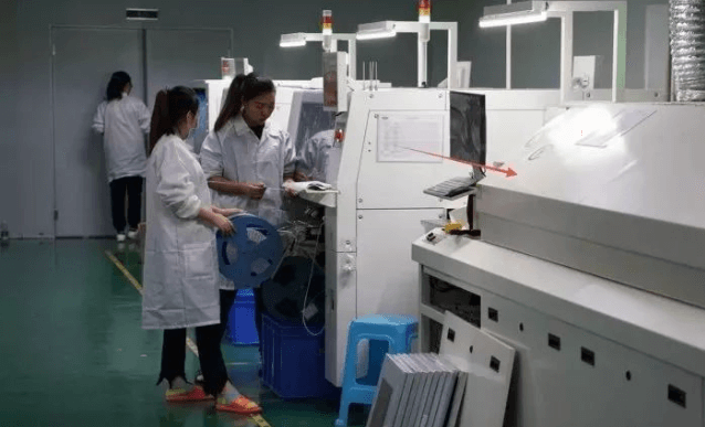
The picture above shows the reflow soldering operation of the lead-free environmental protection process. The one on the right is the reflow soldering equipment, and the internal temperature is as high as more than 200 degrees. There is also a computer on the reflow soldering machine, and the temperature of the reflow soldering machine and the speed of sliding over the PCB board with the material sheet pasted are designed by the program of this computer.
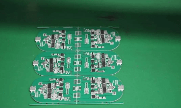
The PCB substrate after brushing paste, patch, and reflow soldering has become a complete PCBA. At this time, the PCBA needs to be inspected, and each part is judged according to the size of the components used in the PCB circuit and the direction of the components. function is normal.
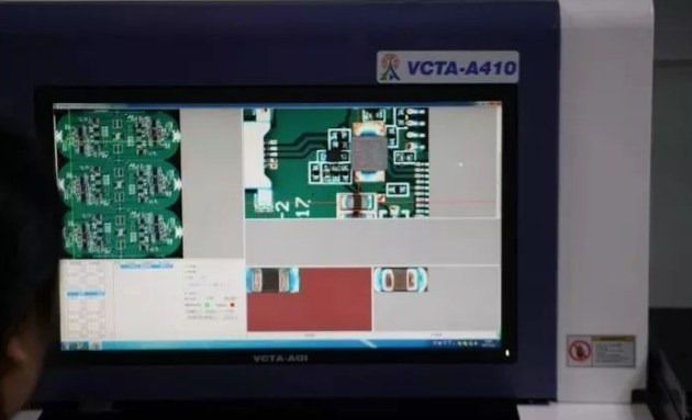
The picture above shows the use of AOI automatic optical detector to inspect the PCBA. Through tens of times of magnification, you can graphically check whether there are problems such as virtual soldering and empty soldering in the process of chip and resistance-capacitance placement.
Lorem ipsum dolor sit amet, consectetur adipiscing elit. Ut elit tellus, luctus nec ullamcorper mattis, pulvinar dapibus leo.
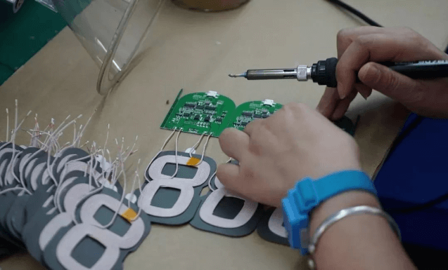
Welding the transmitter coil requires manual operation. It can be seen from the picture that the technician has a blue bracelet on his left hand. There is a wire on the bracelet that is grounded to prevent the human body from breaking down the high-precision chip due to static electricity.
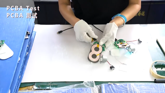
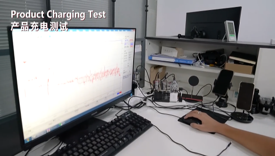
After the PCBA circuit board and the coil are soldered, connect the mobile phone to do a functional test of the semi-finished product.
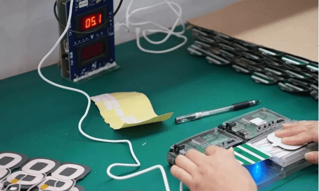
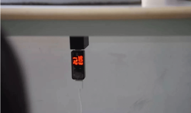
Next, check whether the transmitting coil board is in normal condition. Here, the working conditions of different input voltages will be tested.
The picture shows the voltage and current when the wireless charger is fast charging, 9V/1.7A.
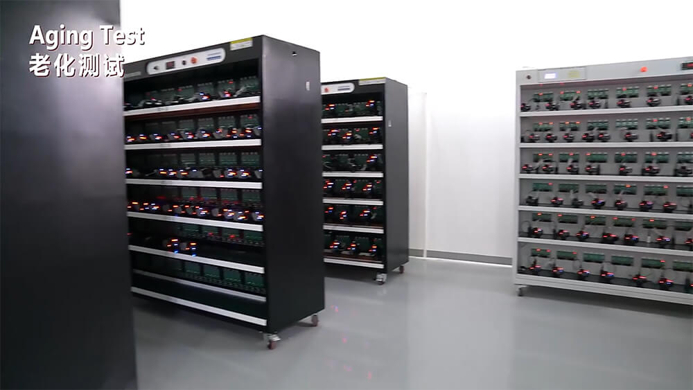
This process is an aging test. Every qualified wireless charger needs power-on and load tests before leaving the factory, so that bad products can be screened out in advance during the test process; those that pass the aging test will enter the assembly process, and the bad ones will be Extract it to troubleshoot the problem. According to the engineer in the factory, the aging test takes 2 hours for single-coil wireless charging, and 4 hours for double-coil wireless charging.
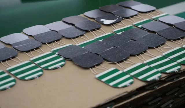
The picture shows the wireless charging circuit board after the aging test, each piece is neatly arranged. The ones with electronic components are facing down to avoid hurting them during the bumping process.
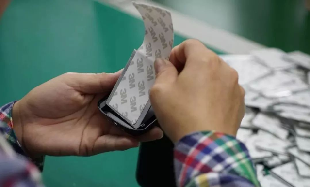

Use 3M glue to fix the transmitter module on the wireless charger shell.
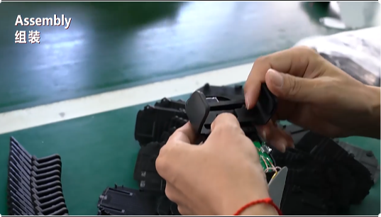
The picture above shows the semi-finished wireless charger that has been assembled and is about to wait for the next assembly link.
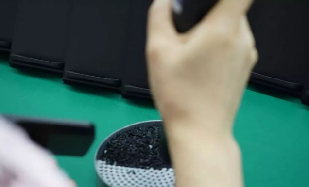
Put on the screws. A vertical wireless charger with dual-coil fast charging is assembled.
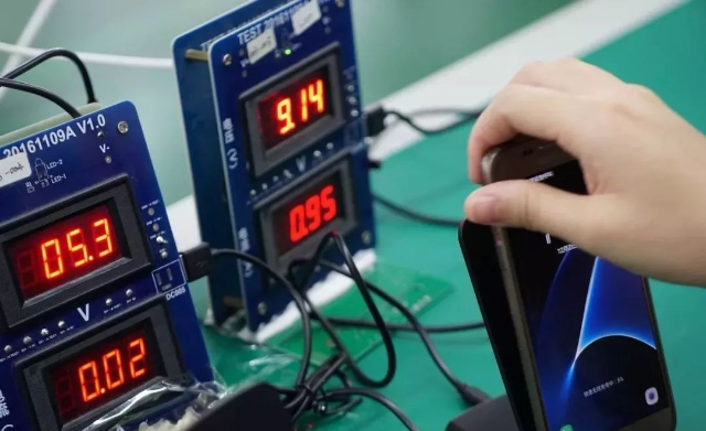
The real phone test before leaving the factory, it can be seen from the picture that it is a Samsung wireless charging mobile phone. This link is used to rule out the compatibility of wireless charging to ensure that the wireless charging products that arrive at the user’s hands can have the same performance experience as the original charger.
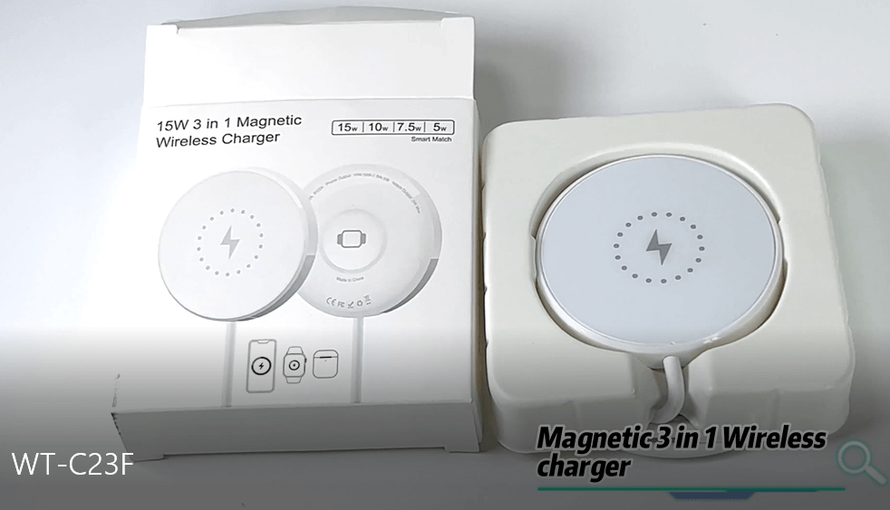
Pack the wireless charger with an adsorbed plastic box and color box. The adsorbed plastic box is customized according to the model of the product. The adsorbed plastic box improves the protection of the wireless charger during transportation. Packed in boxes and distributed all over the world. The wireless charger body and packaging factory can also make private customized LOGO, and various wireless charging products are displayed in the exhibition hall of the manufacturer.
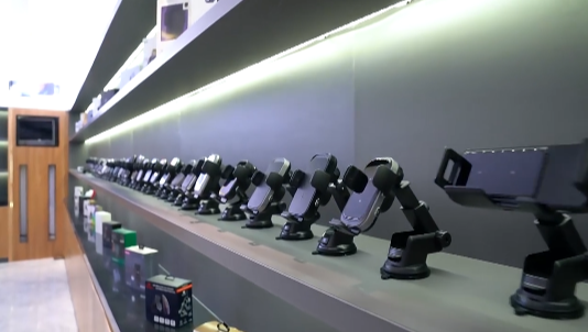
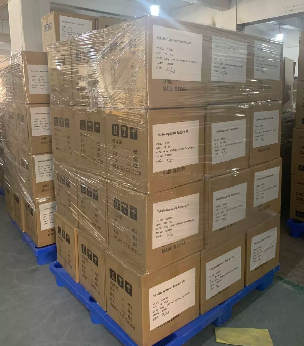
These are the complete production process of wireless charging. In short, it is appearance design, shell injection mold opening, plastic manufacturing, PCB board circuit design, PCB printing, SMT machine placement, reflow soldering, AI machine PCBA inspection, manual welding of PCBA and coil, Semi-finished product inspection, aging test, gluing, shell assembly, finished product testing, finished product packaging. the In order to ensure the safety and reliability of our products, we will carry out mold testing, performance testing of electronic functions, visual inspection, etc. for wireless charging.
After reading it, do you have a detailed understanding of the mysterious wireless charging production process? For more details or cooperation, please contact INPUT, we will serve you one-on-one within 24 hours.

Regarding the Wireless CarPlay adapter, let’s first understand CarPlay. What is Carplay? In the center console of a car, there
1-1-300x152.jpg)
Dear partners and customers, We sincerely invite you to participate in the 2024 Spring Hong Kong Electronics Exhibition. As a
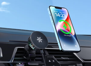
magnetic car holders in themselves do not disrupt wireless charging, unless the specific design places the magnet too close to
Phone: 0086-755-89812186
Email: sales@inputcn.com
Address: 518129 2F Building 1, Baoli Industrial Zone,
Bantian, Longgang District, Shenzhen, China.

